- 您现在的位置:买卖IC网 > Sheet目录3890 > PIC18C858T-I/PT (Microchip Technology)IC MCU OTP 16KX16 CAN 80TQFP
2000 Microchip Technology Inc.
Advanced Information
DS30475A-page 101
PIC18CXX8
8.7
PORTG, LATG, and TRISG Registers
PORTG is a 5-bit wide, bi-directional port. The corre-
sponding Data Direction register is TRISG. Setting a
TRISG bit (=1) will make the corresponding PORTG pin
an input (i.e., put the corresponding output driver in a
hi-impedance mode). Clearing a TRISG bit (=0) will
make the corresponding PORTG pin an output (i.e., put
the contents of the output latch on the selected pin).
Read-modify-write operations on the LATG register
read and write the latched output value for PORTG.
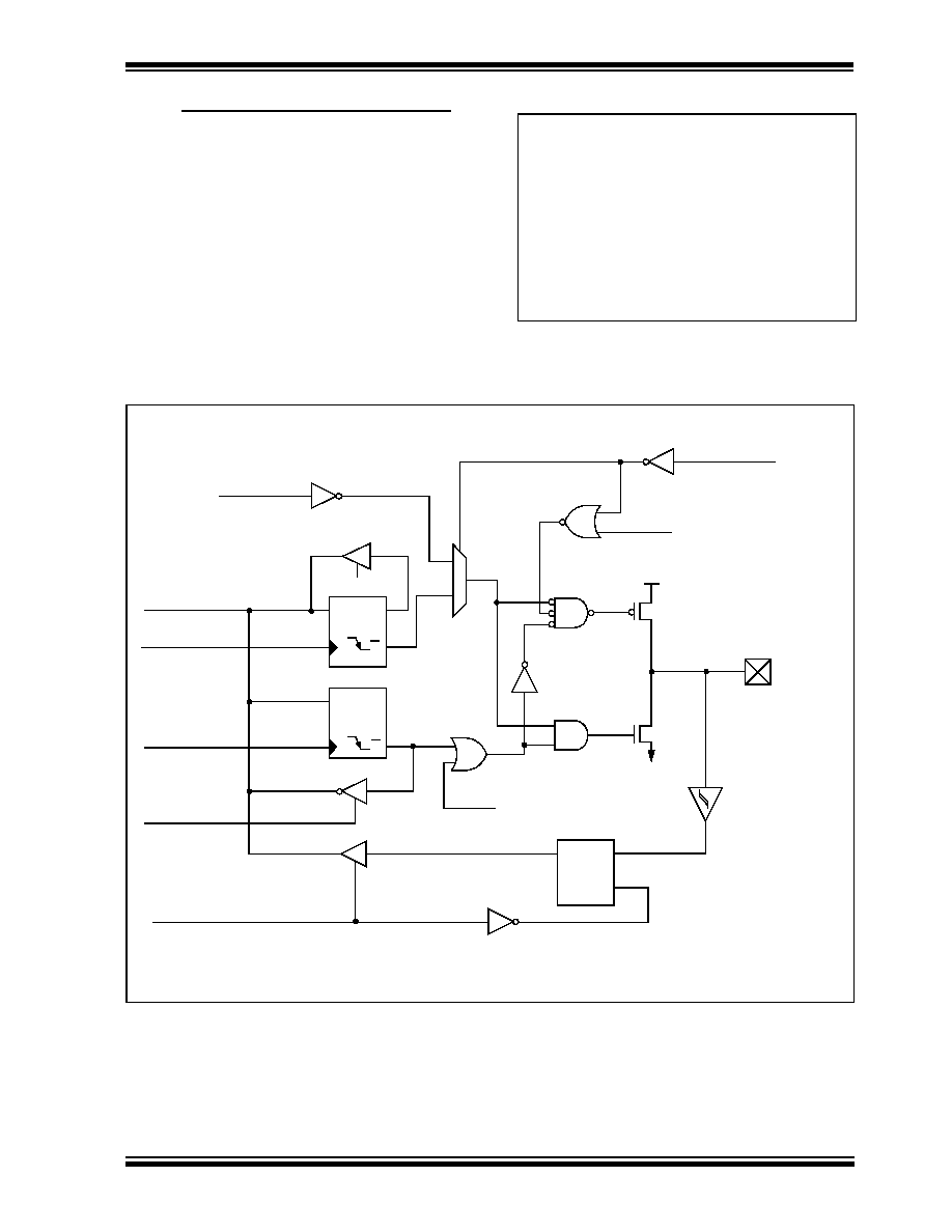
Pins RG0-RG2 on PORTG are multiplexed with the
CAN peripheral. Refer to "CAN Module", Section 17.0
for proper settings of TRISG when CAN is enabled.
EXAMPLE 8-7:
INITIALIZING PORTG
FIGURE 8-12: RG0/CANTX0 PIN BLOCK DIAGRAM
CLRF
PORTG
; Initialize PORTG by
; clearing output
; data latches
CLRF
LATG
; Alternate method
; to clear output
; data latches
MOVLW
0x04
; Value used to
; initialize data
; direction
MOVWF
TRISG
; Set RG1:RG0 as outputs
; RG2 as input
; RG4:RG3 as outputs
Data
Latch
TRIS Latch
RD TRISG
P
VSS
Q
D
Q
CK
Q
D
Q
CK
EN
QD
EN
N
VDD
0
1
RD PORTG
WR TRISG
Data Bus
I/O Pin
TXD
ENDRHI
OPMODE2:OPMODE0=000
Schmitt
Trigger
RD LATG
WR PORTG or
WR LATG
OPMODE2:OPMODE0 = 000
Note:
I/O pins have diode protection to VDD and VSS.
发布紧急采购,3分钟左右您将得到回复。
相关PDF资料
PIC18C658T-I/PT
IC MCU OTP 16KX16 CAN 64TQFP
PIC16LC717T-E/SS
IC MCU OTP 2KX14 A/D PWM 20SSOP
PIC16LC771T/SO
IC MCU OTP 4KX14 A/D PWM 20SOIC
PIC16LC771T-E/SO
IC MCU OTP 4KX14 A/D PWM 20SOIC
PIC16C771T-E/SO
IC MCU OTP 4KX14 A/D PWM 20SOIC
PIC16LC770T/SS
IC MCU OTP 2KX14 A/D PWM 20SSOP
PIC16LC717T-I/SO
IC MCU OTP 2KX14 A/D PWM 18SOIC
PIC16LC771T/SS
IC MCU OTP 4KX14 A/D PWM 20SSOP
相关代理商/技术参数
PIC18F1220-E/ML
功能描述:8位微控制器 -MCU 4KB 256 RAM 16 I/O RoHS:否 制造商:Silicon Labs 核心:8051 处理器系列:C8051F39x 数据总线宽度:8 bit 最大时钟频率:50 MHz 程序存储器大小:16 KB 数据 RAM 大小:1 KB 片上 ADC:Yes 工作电源电压:1.8 V to 3.6 V 工作温度范围:- 40 C to + 105 C 封装 / 箱体:QFN-20 安装风格:SMD/SMT
PIC18F1220-E/P
功能描述:8位微控制器 -MCU 4KB 256 RAM 16 I/O RoHS:否 制造商:Silicon Labs 核心:8051 处理器系列:C8051F39x 数据总线宽度:8 bit 最大时钟频率:50 MHz 程序存储器大小:16 KB 数据 RAM 大小:1 KB 片上 ADC:Yes 工作电源电压:1.8 V to 3.6 V 工作温度范围:- 40 C to + 105 C 封装 / 箱体:QFN-20 安装风格:SMD/SMT
PIC18F1220-E/SO
功能描述:8位微控制器 -MCU 4KB 256 RAM 16 I/O RoHS:否 制造商:Silicon Labs 核心:8051 处理器系列:C8051F39x 数据总线宽度:8 bit 最大时钟频率:50 MHz 程序存储器大小:16 KB 数据 RAM 大小:1 KB 片上 ADC:Yes 工作电源电压:1.8 V to 3.6 V 工作温度范围:- 40 C to + 105 C 封装 / 箱体:QFN-20 安装风格:SMD/SMT
PIC18F1220-E/SS
功能描述:8位微控制器 -MCU 4KB 256 RAM 16 I/O RoHS:否 制造商:Silicon Labs 核心:8051 处理器系列:C8051F39x 数据总线宽度:8 bit 最大时钟频率:50 MHz 程序存储器大小:16 KB 数据 RAM 大小:1 KB 片上 ADC:Yes 工作电源电压:1.8 V to 3.6 V 工作温度范围:- 40 C to + 105 C 封装 / 箱体:QFN-20 安装风格:SMD/SMT
PIC18F1220-H/ML
功能描述:8位微控制器 -MCU 4KB FL 256RAM 16 I/O RoHS:否 制造商:Silicon Labs 核心:8051 处理器系列:C8051F39x 数据总线宽度:8 bit 最大时钟频率:50 MHz 程序存储器大小:16 KB 数据 RAM 大小:1 KB 片上 ADC:Yes 工作电源电压:1.8 V to 3.6 V 工作温度范围:- 40 C to + 105 C 封装 / 箱体:QFN-20 安装风格:SMD/SMT
PIC18F1220-H/P
功能描述:8位微控制器 -MCU 4KB FL 256RAM 16 I/O RoHS:否 制造商:Silicon Labs 核心:8051 处理器系列:C8051F39x 数据总线宽度:8 bit 最大时钟频率:50 MHz 程序存储器大小:16 KB 数据 RAM 大小:1 KB 片上 ADC:Yes 工作电源电压:1.8 V to 3.6 V 工作温度范围:- 40 C to + 105 C 封装 / 箱体:QFN-20 安装风格:SMD/SMT
PIC18F1220-H/SO
功能描述:8位微控制器 -MCU 4KB FL 256RAM 16 I/O RoHS:否 制造商:Silicon Labs 核心:8051 处理器系列:C8051F39x 数据总线宽度:8 bit 最大时钟频率:50 MHz 程序存储器大小:16 KB 数据 RAM 大小:1 KB 片上 ADC:Yes 工作电源电压:1.8 V to 3.6 V 工作温度范围:- 40 C to + 105 C 封装 / 箱体:QFN-20 安装风格:SMD/SMT
PIC18F1220-H/SS
功能描述:8位微控制器 -MCU 4KB FL 256RAM 16 I/O RoHS:否 制造商:Silicon Labs 核心:8051 处理器系列:C8051F39x 数据总线宽度:8 bit 最大时钟频率:50 MHz 程序存储器大小:16 KB 数据 RAM 大小:1 KB 片上 ADC:Yes 工作电源电压:1.8 V to 3.6 V 工作温度范围:- 40 C to + 105 C 封装 / 箱体:QFN-20 安装风格:SMD/SMT